
Most Advanced Tabletop Laser Direct Imager
Flexible direct imaging solutions for rapid microfabrication, R&D patterning, and fast design iteration — from economical tabletop systems to high-end sub-micron semiconductor platforms — without conventional mask turnaround.

Direct Patterning for R&D
Laser Direct Imager systems help research teams move quickly from CAD designs to patterned substrates, making them useful for MEMS, sensors, microfluidics, and academic prototyping.
By eliminating the need for physical photomasks, these systems dramatically reduce prototyping time and cost while keeping the workflow fully software-driven.
High-End Laser Direct Writer
Our high-end Laser Direct Writers (LDW) deliver exceptional resolution and throughput for demanding semiconductor and research applications.
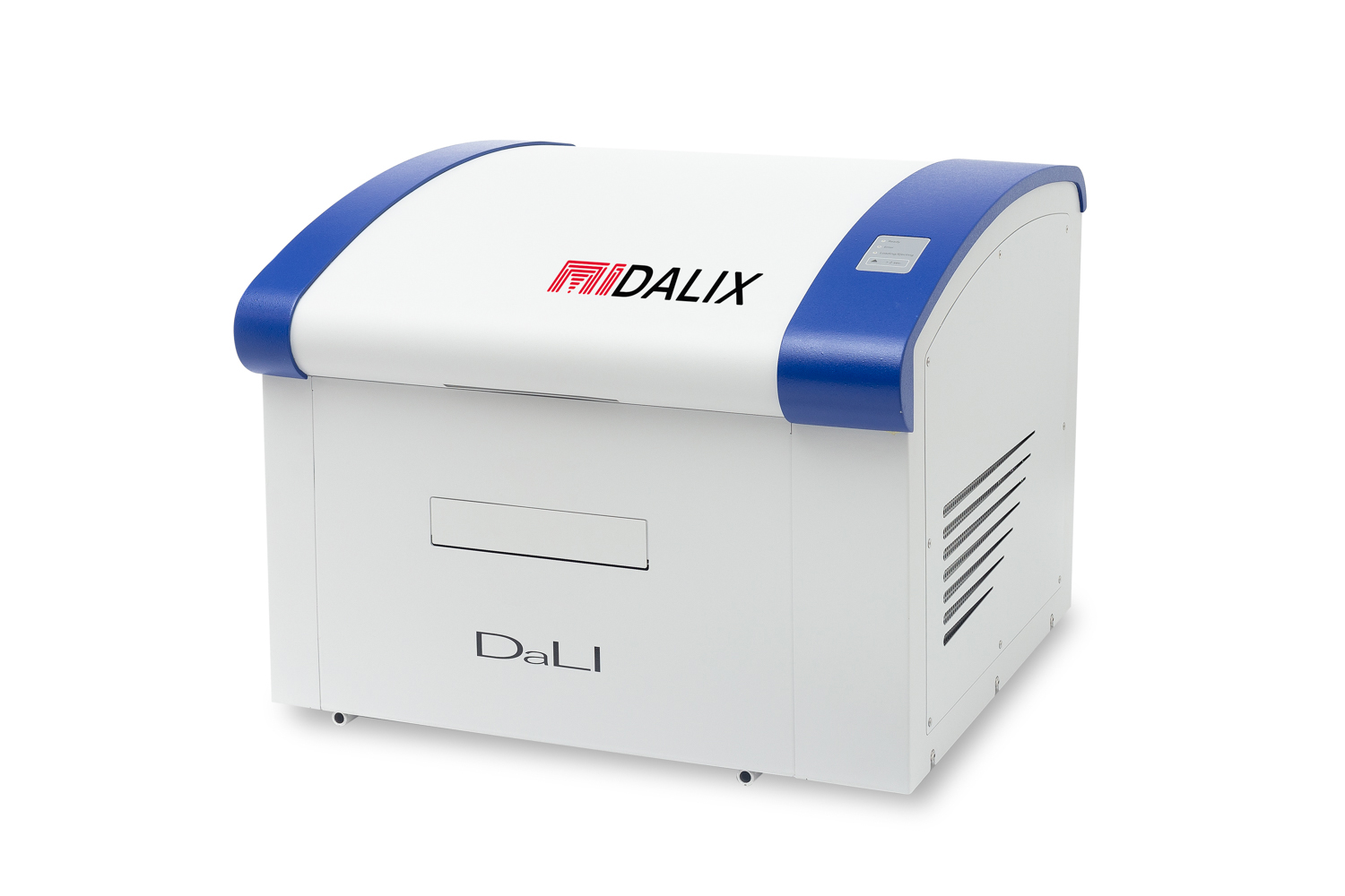
Dali a state of the art and most advanced Table-top Laser Direct Imager, using a precisely guided laser source for the illumination of lithographic patterns / structures. Maskless lithography features make design changes a breeze, since it eliminates the highly sensitive step of sample to mask alignment and saves both time and money in the process. Transfers computer-generated digital patterns onto a photoresist-coated substrate without requiring a physical photomask. Laser Direct Imager extensively used in applications in semiconductor fabrication, micro-electro-mechanical systems (MEMS), photonics, energy storage systems, and optoelectronic components.
Dali allows rapid prototyping in-house at no extra cost for expensive Photomask. Write the sample directly from the computer with precise alignment accuracy in nm. It offers Ultra precision resolution, Quick turnaround, low cost for Prototype, small batch production, In house fabrication, etc.
Suitable with all standard photoresists and can write planar, non-planar, flexible surfaces and any type of substate.
Acousto-optic deflectors (AOD) for ultra precision
Acousto-optic deflectors (AOD) in combination with a stabilized laser source, complete with thermal stabilization makes lithography process a breeze. Illumination resolution far below 1µm, implemented by a near-UV laser source paired with acousto-optic deflectors (AOD) for quick and precise laser beam guiding, rapidly illuminating structures with nanometer precision on the material. The high light intensity is achieved by using a laser source enables fast movement between regions of the sample according to structure design, without any moving parts. The AOD makes use of the effect of sound waves on light propagation. A high frequency piezoelectric transducer attached to one side of an AOD crystal induces ultra-sonic waves inside the crystal, causing multiple reflections of an incident electromagnetic plane wave. The ultra-sonic waves appear as static for the incoming laser beam as electromagnetic waves travel much faster than acoustic waves. The system has only a few moving mechanical parts, thus resulting in excellent operating life and incomparable deflecting speeds and resolution. The deflection angle is linearly related to the frequency of the acoustic wave inside the AOD crystal.
Software driven
The Dali is fully software driven and it covers all aspects of machine operation, from setup, calibration, CAD and optimized illumination algorithms, till the sample is completed and ejected. It is comprehensive and enables direct write lithography on Micrometer sized samples, with structures precisely aligned on existing features. Our CAD library allows designing from scratch or modifications of partially or fully ready patterns even on a standalone PC without the DaLI system connected. Import filters can import design in dxf and bmp formats. One can assign different illumination parameters to individual parts of structures, e.g. the diameter of laser beam, the illumination dose, the illumination resolution, mode, and place of stitching the fields and many more. By employing an integrated microscope 20x, it is possible to level the substrate to bring its surface into laser focus, determine the location of eventual related patterns or objects, perform various geometric measurements, etc.
User-friendly
Direct to processing regimes, one button operation and automated sample placement and focusing.
Key features:
Substate size < 100x100mm
Nanometer precision inside a single illumination field
Avoid Alignment errors.
100,000 random dots per second illuminated employing AOD
Repeatability with accuracy
Permits immediate design modifications
100 Greyscale illumination
5 axis positioning of substrate for automatic levelling
CAD with DXF and BMP import filters implemented
Temperature controlled by Solid State Chiller for optical performance.
Small foot print on a table top operation.
Real-time monitoring.
Economical Tabletop System
A budget-conscious instrument that keeps the core architecture and user-friendly operation of a direct imaging system while optimizing specifications for budget-conscious laboratories and academic environments.
For standard R&D patterning tasks.
Fast design-to-exposure iteration.
For teaching labs and prototype facilities.
With most of the above features with writing size of 25mm x 25mm & ~ 3µm feature size with reduced options. Please contact for further details.
Research Domains
Accelerating development in microfabrication and nanotechnology.
Semiconductor / Microelectronics / HDI / MEMS / PCB
Projects computer-aided design data directly onto photosensitive layers. It bypasses physical photomasks to achieve high-precision patterning for advanced IC packaging substrates.
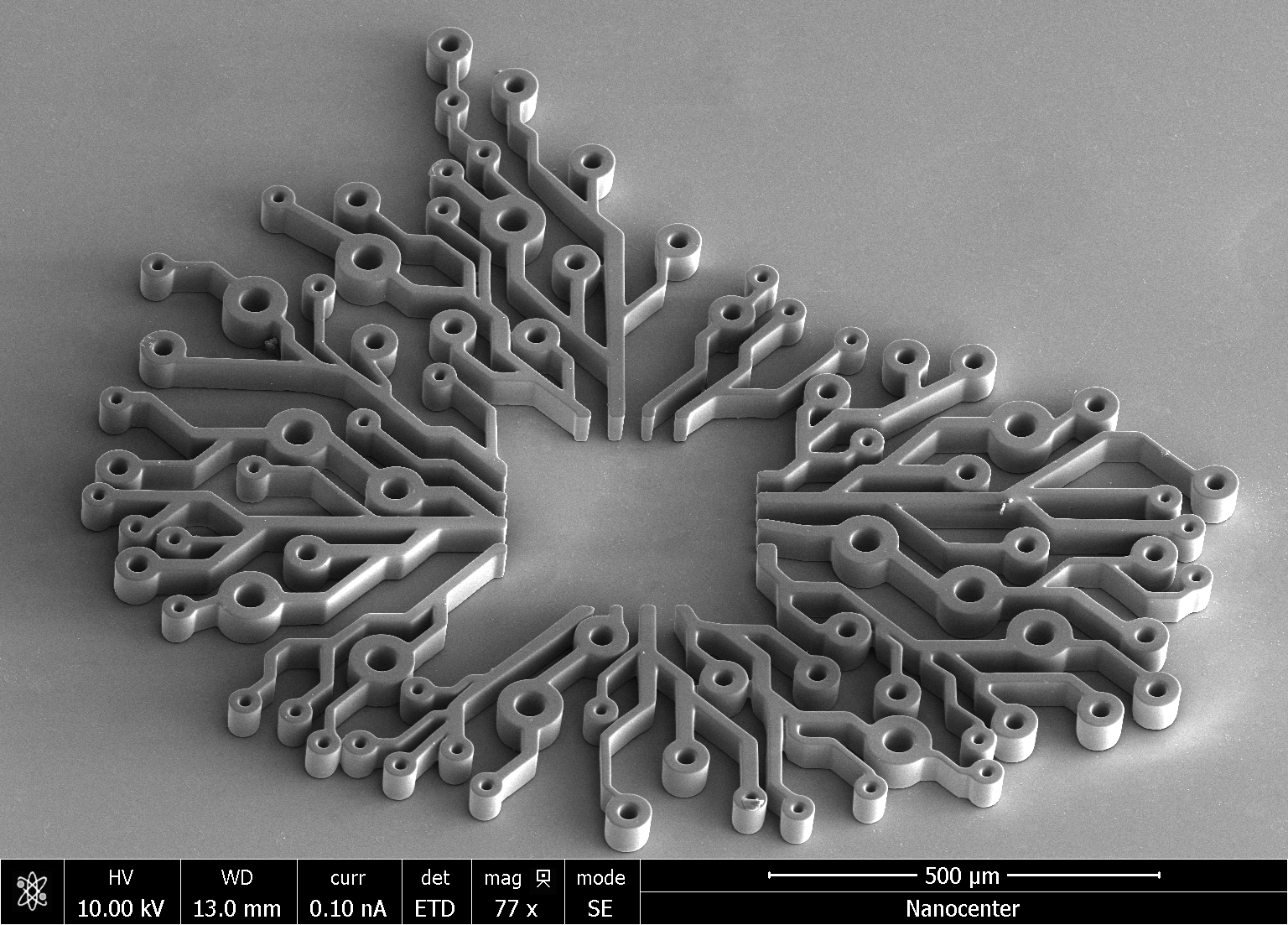
High-density interconnect (HDI) boards, Flexible and rigid-flex PCBs, Dense PCBs and simple chip designs with precise alignment can be realized through a combination of lithographic steps and further chemical or other processing steps. Simple silicon chip designs can be tested on whole wafer substrates, as holders can be exchanged for 2” to 4” diameters. DaLI supports standard photoresist materials, offering an option to integrate into existing prototyping and manufacturing facilities.
Lithographic structures can be prepared on virtually any material with sufficiently low roughness, either directly or with the help of bonding agents in the form of sputtered thin metal layers or dried chemicals. Lithography serves for either creating a mask for further etching steps (i.e. for silicon-based MEMS) or for direct structuring of thick photoresists, creating mechanical components made of photoresist materials. High precision and repeatability are necessary for reliable micromechanical components, both delivered by DaLI’s Acoustio Optic Deflectors (AOD) with integrated control systems. High aspect ratio microstructures, such as gears, mixers and valves, can be created through the use of the coarse tool setting, enlarging the vertical reach, but keeping walls smooth. LDI improves precision and reduces distortion in pattern transfer in a PCB.
Material Science, 2D Materials and Quantum devices
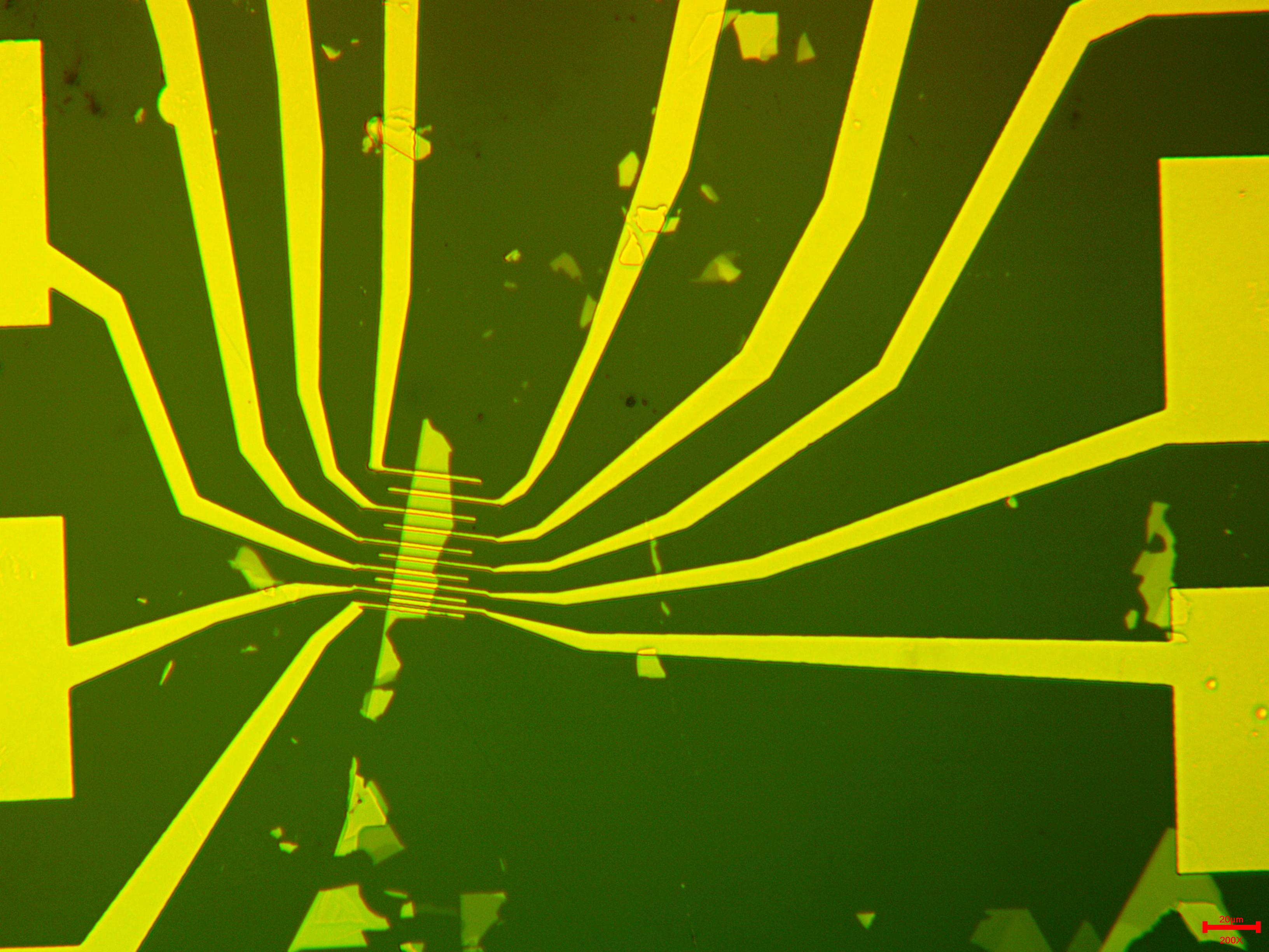
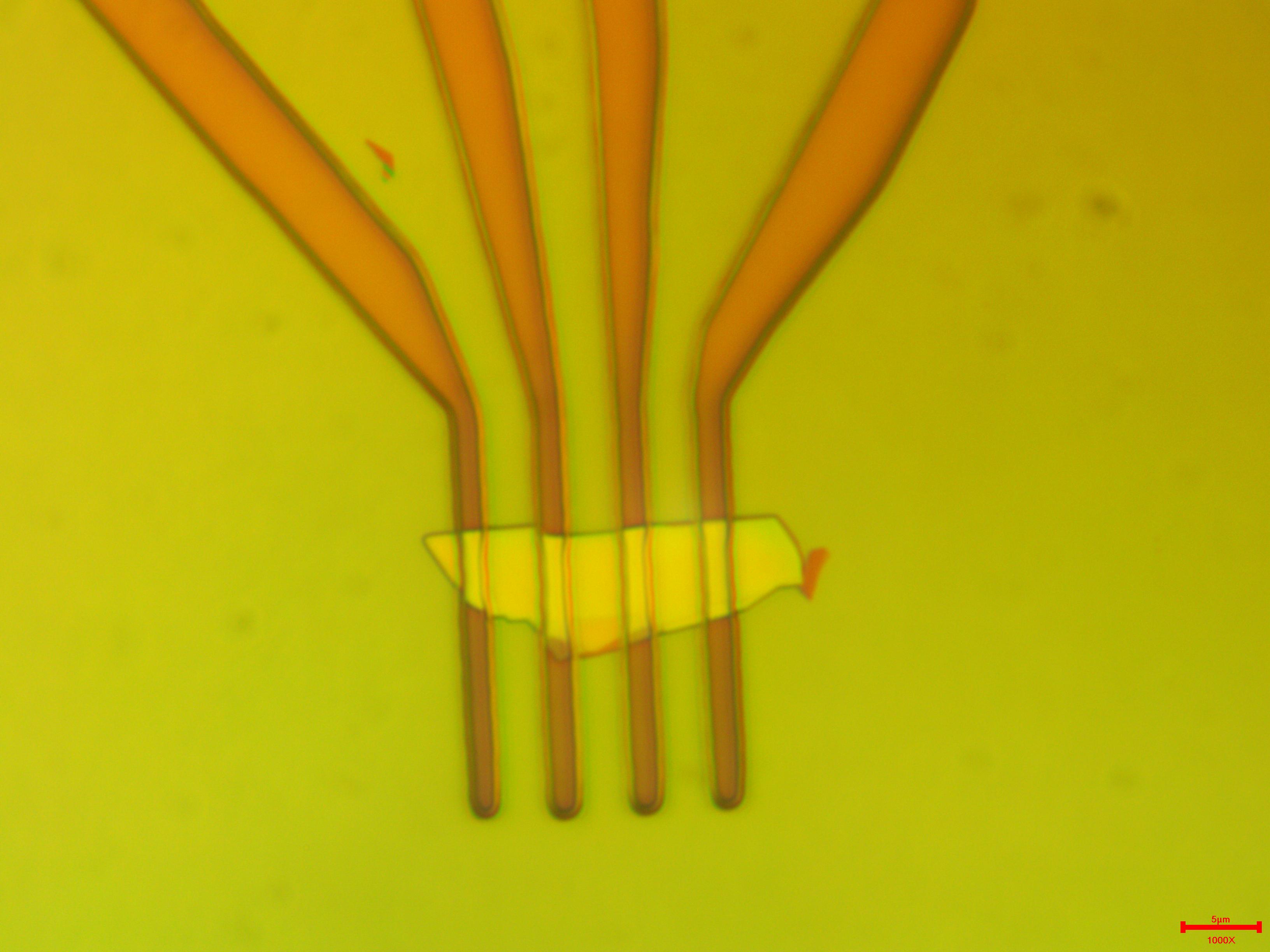
Various electrodes and other designs can be transferred to a single micro crystal, mono layers and other demanding surfaces. With laser lithography various electrodes and other designs can be transferred to a single micro crystal, mono layers and other demanding surfaces.
Precise, nm resolution design with smooth edges and sub micrometer features can be realized Accurate positioning and designs of structures based on targeted object’s (crystal, fiber, flake) position, shape and size are possible — markers or additional alignment features are not required.
Candidates and their thickness (crystals, flakes etc.) can be identified and differentiated in situ employing color microscope integrated
Microfluidics
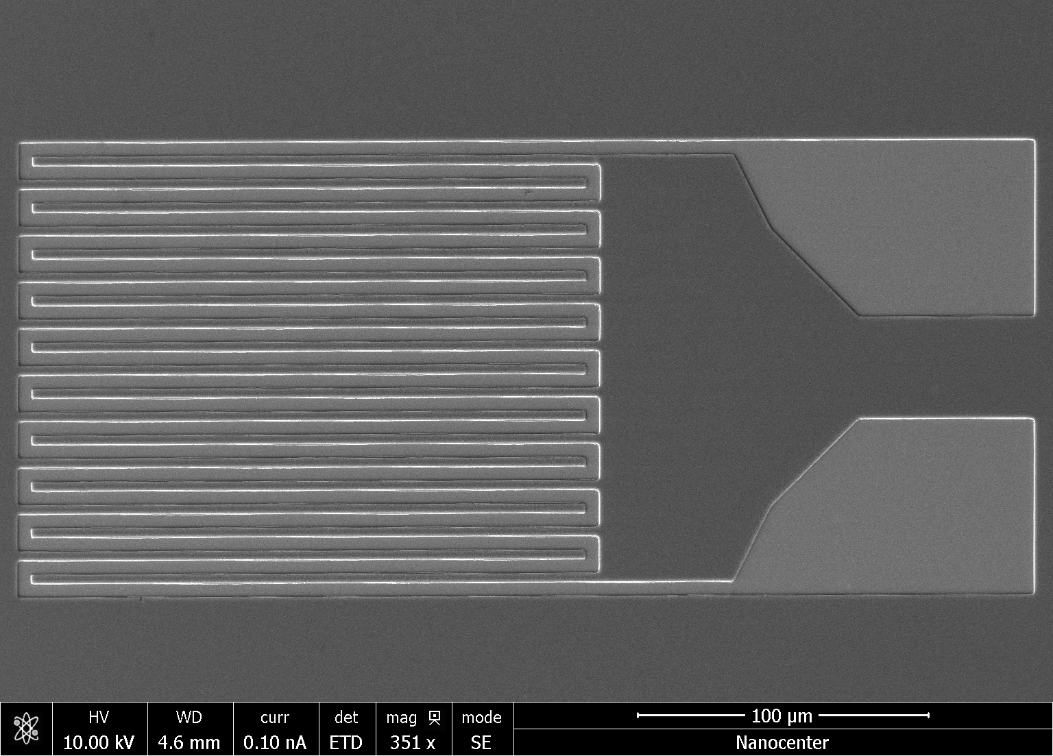
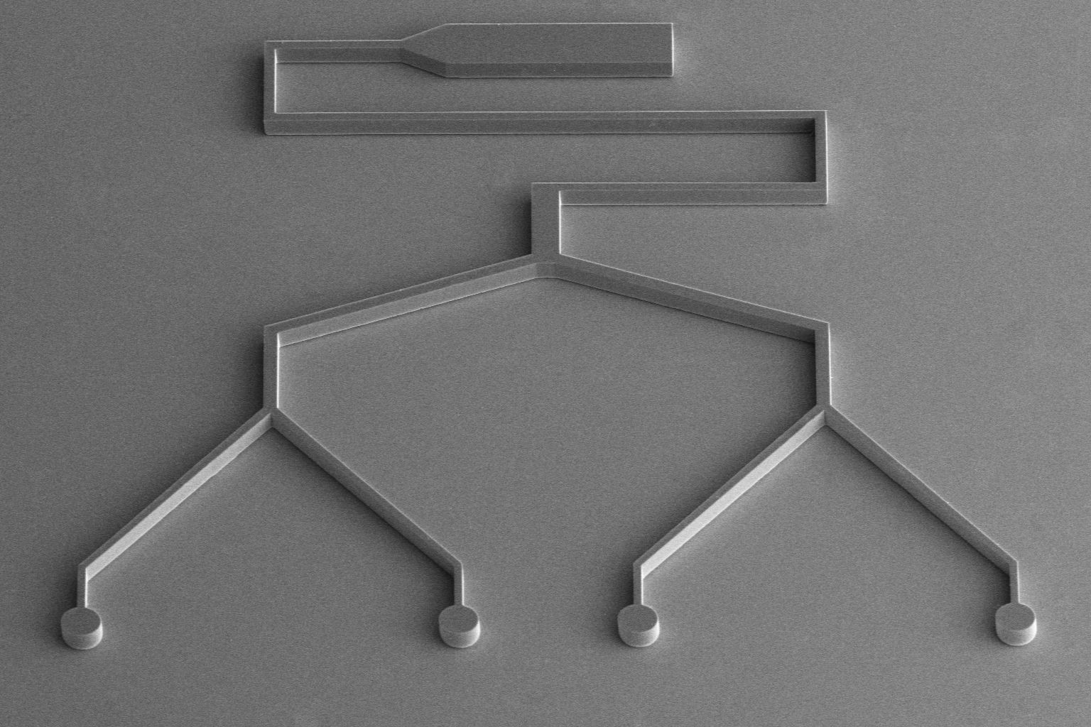
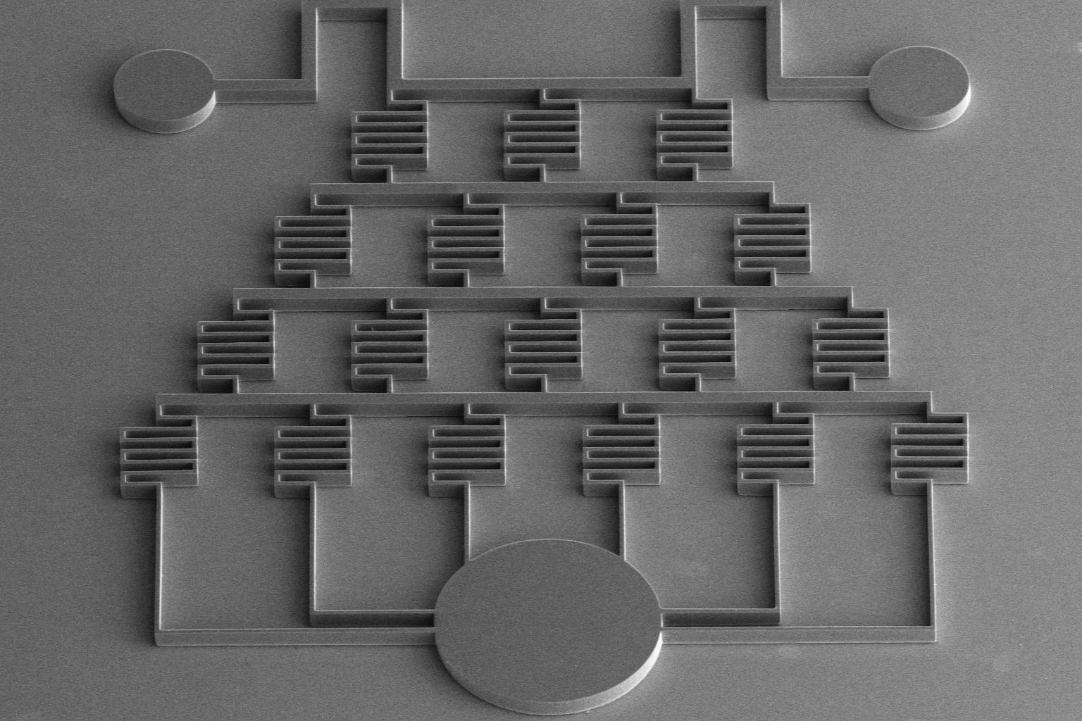
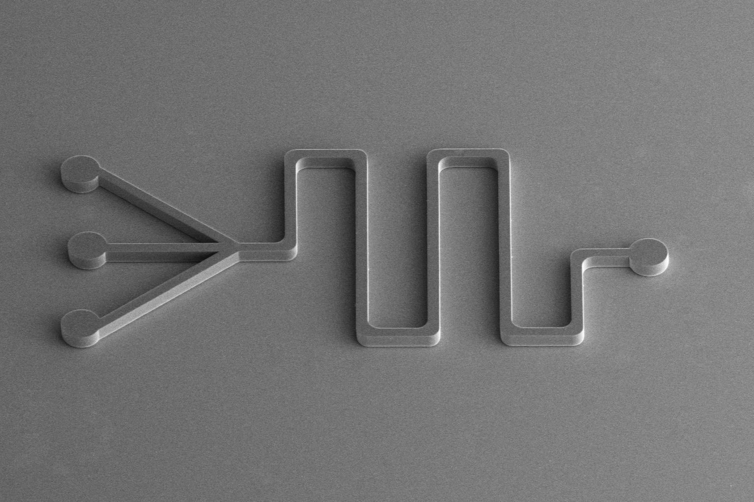
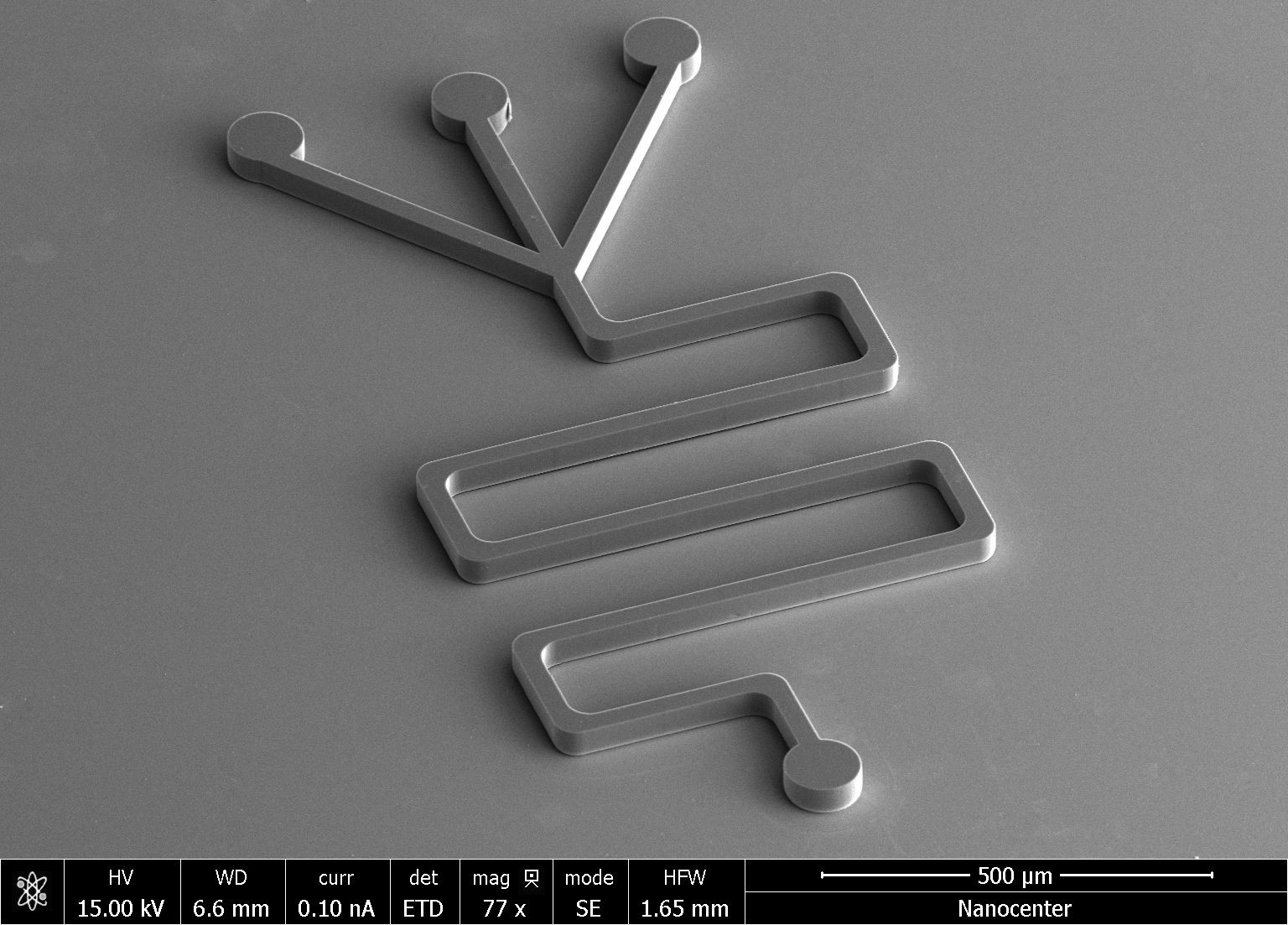
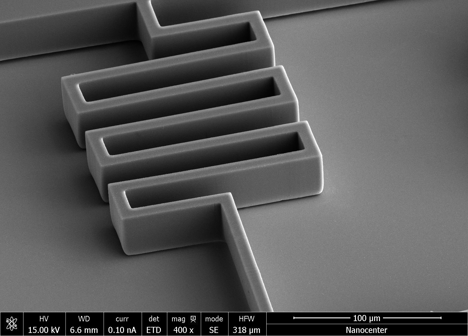
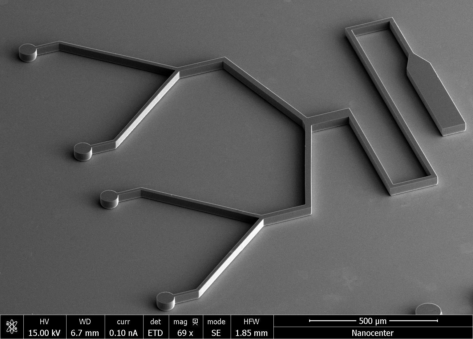
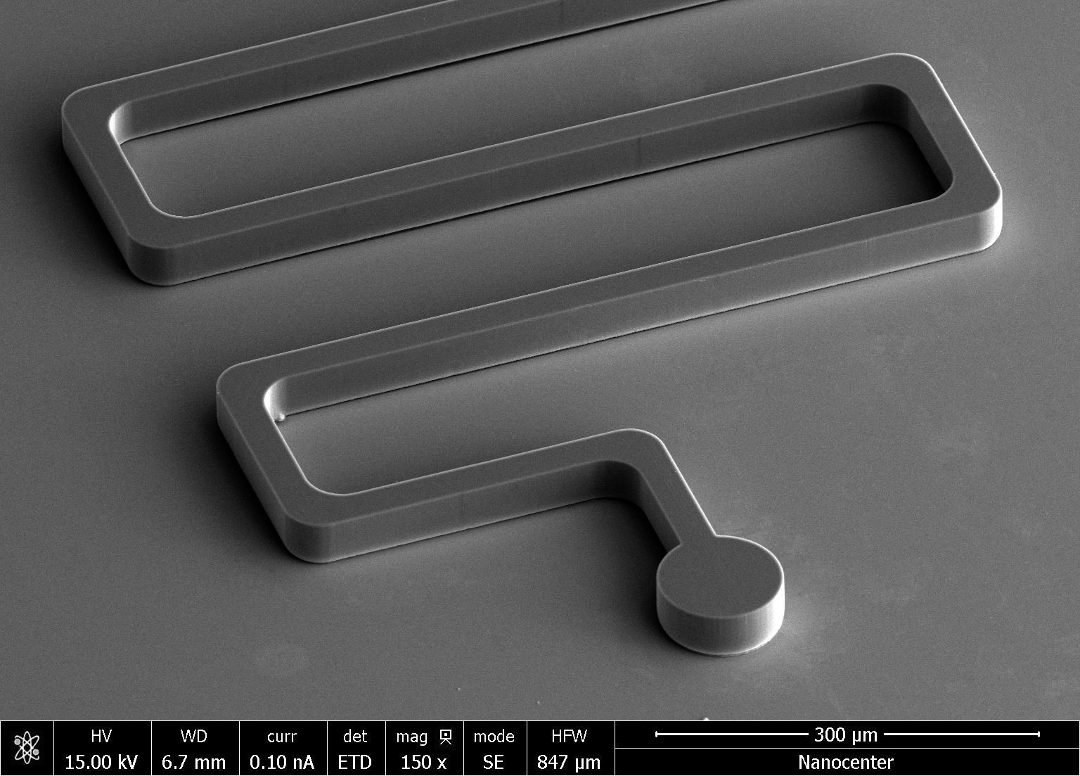
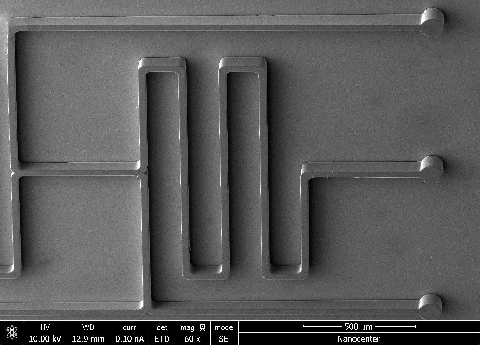
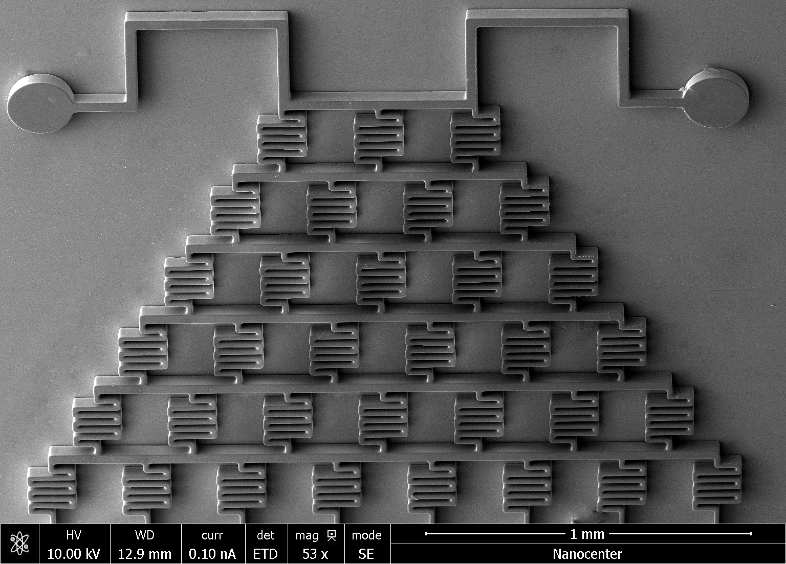
Microfluidic customized channels embossed in PDMS or similar materials can exhibit high-aspect ratios, smooth walls, and well-defined corners, as well as potentially structured walls to manipulate flows of liquids or particles. Our coarse tool offers higher processing speeds compared to fine tool as a consequence of using a larger laser spot size on material but achieves equally smooth channel wall as well as minimal deviations from vertical sides in case of thick photoresists.
Large overall scale, demanded due to necessary connections to external pumps and reservoirs, is quickly achieved with the use of the coarse tool. Large scale structures and single micrometer scale channels are seamlessly connected with automated stitching. Pattern photosensitive Biological Scaffolds, Tissue Engineering or microfluidic channels with micrometer-level precision.
Lab-on-a-Chip device
Miniaturized laboratories, enabling various biological or chemical reactions taking place on a mm-cm scale substrate, are already a staple for in-situ detection methods and diagnostics in remote areas. Multiple laboratory functions need to be integrated on a single lab-on-a-chip device, often combining Microfluidics, Micromechanical and Micro electrical components, thus facilitating the need of controlled Centimeter scale structuring with the ability to define Micrometer scale details. Also for Cell sorting applications.
Highly precise lithographic structures are needed for a high-quality final device, in order to avoid leaks and jams in the contained flows. Non-contact methods of sample mounting, positioning, and structure illumination in DaLI serve to maintain a clean microscale environment.
Biosensor / Wearable Health Monitors
Green Laser-Induced Graphene (LIG) is a sustainable technology that uses direct laser writing to convert renewable bio-based materials—such as lignin, chitosan, and cork—into porous, conductive graphene. This eco-friendly method replaces standard synthetic plastic precursors with natural carbon sources to build flexible electronics and Biosensors. various inexpensive flexible polymer substrates, mainly polyimide are scribed through laser irradiation and Laser Induced Graphene (LIG) materials are produced Laser-induced graphene (LIG) sensors are flexible, porous carbon devices made by using a laser to turn polymer films (like polyimide) into graphene. They measure physical and chemical changes, feature a fast, low-cost production method, and work well for wearable health monitors. Sensors can be drawn right onto a flexible base directly without any Photomask.
Biophysics
Photoresist materials can either directly serve as a base layer for biophysical experiments, with surfaces modified through lithographic steps, or can be used to emboss the textured surface to other biocompatible materials. Photoresist surface texturing is achieved with precise control of illumination parameters, resulting in various textures exhibiting different physical properties to control flows, biocompatibility, or friction.
Hierarchically organized surface structures and single-micron scale two-dimensional array patterns, both realized in thin photoresists, act as in-vitro simulations of real life complex biological systems.
Thermochemical
Is increasingly employed as a thermochemical tool for direct material conversion, such as localized pyrolysis. This method utilizes renewable and low-cost lignin as a carbon precursor, which undergoes localized pyrolysis through laser irradiation to successfully fabricate 3D porous lignin-derived laser-induced graphene (LSG). Irradiate the targeted areas of the lignin film; high localized heat vaporizes volatile gases and rearranges the aromatic lignin structures into a conductive, 3D hierarchically porous graphene network. Fabricated 3D graphene electrodes on the surface of lignin films by laser in situ writing, which opens up a new way for large-scale and low-cost manufacturing of flexible electronic devices and micro supercapacitors
Latest Works
 Lab on a Chip
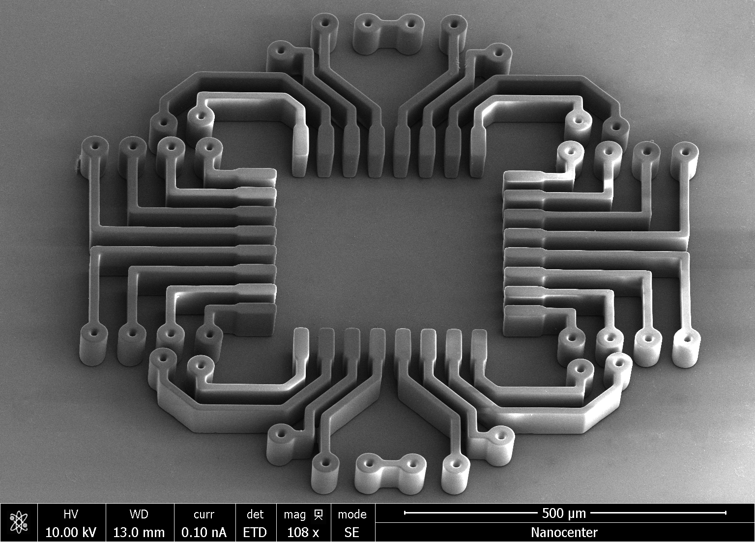 Lab on a Chip
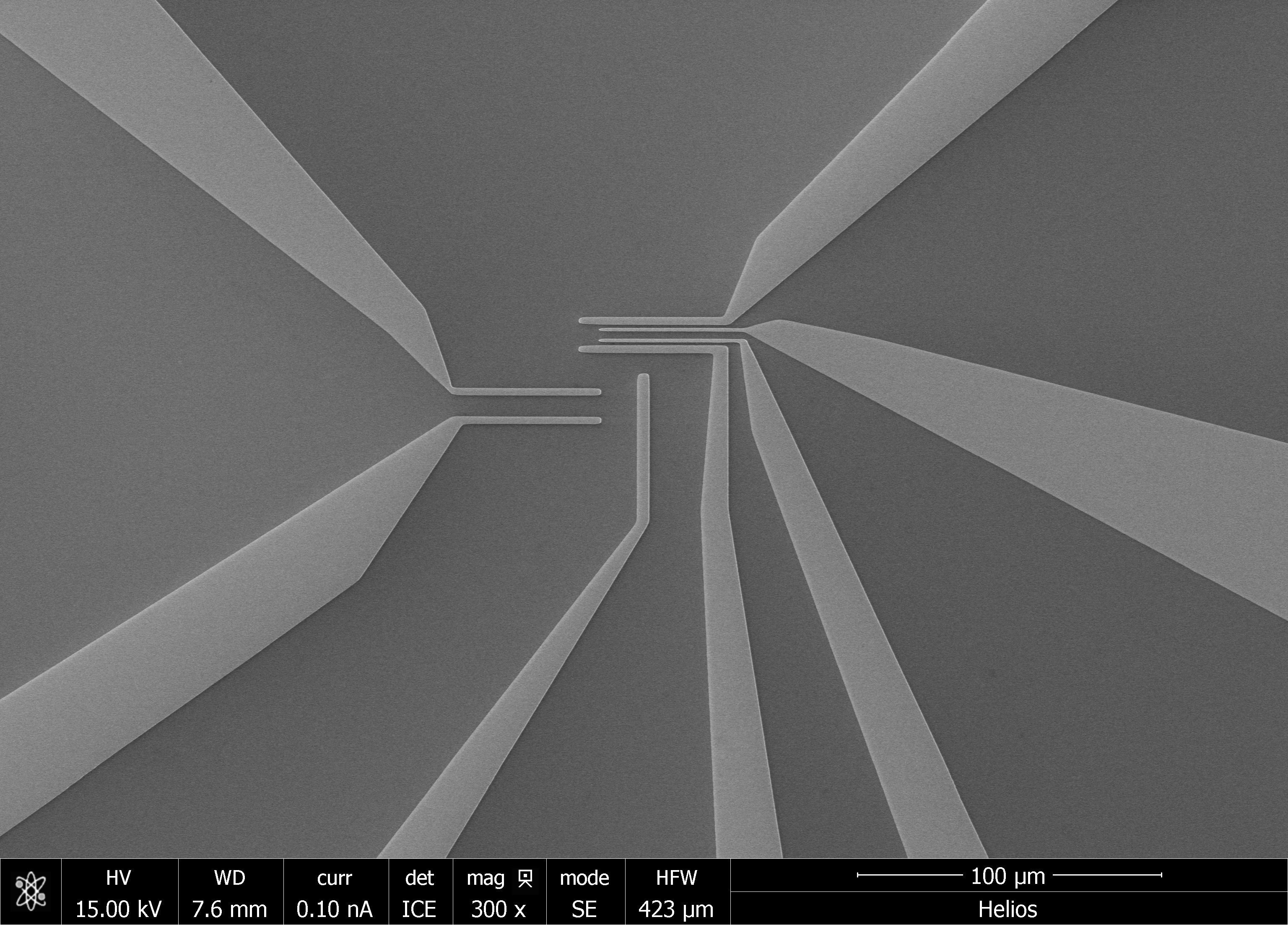 Material Science
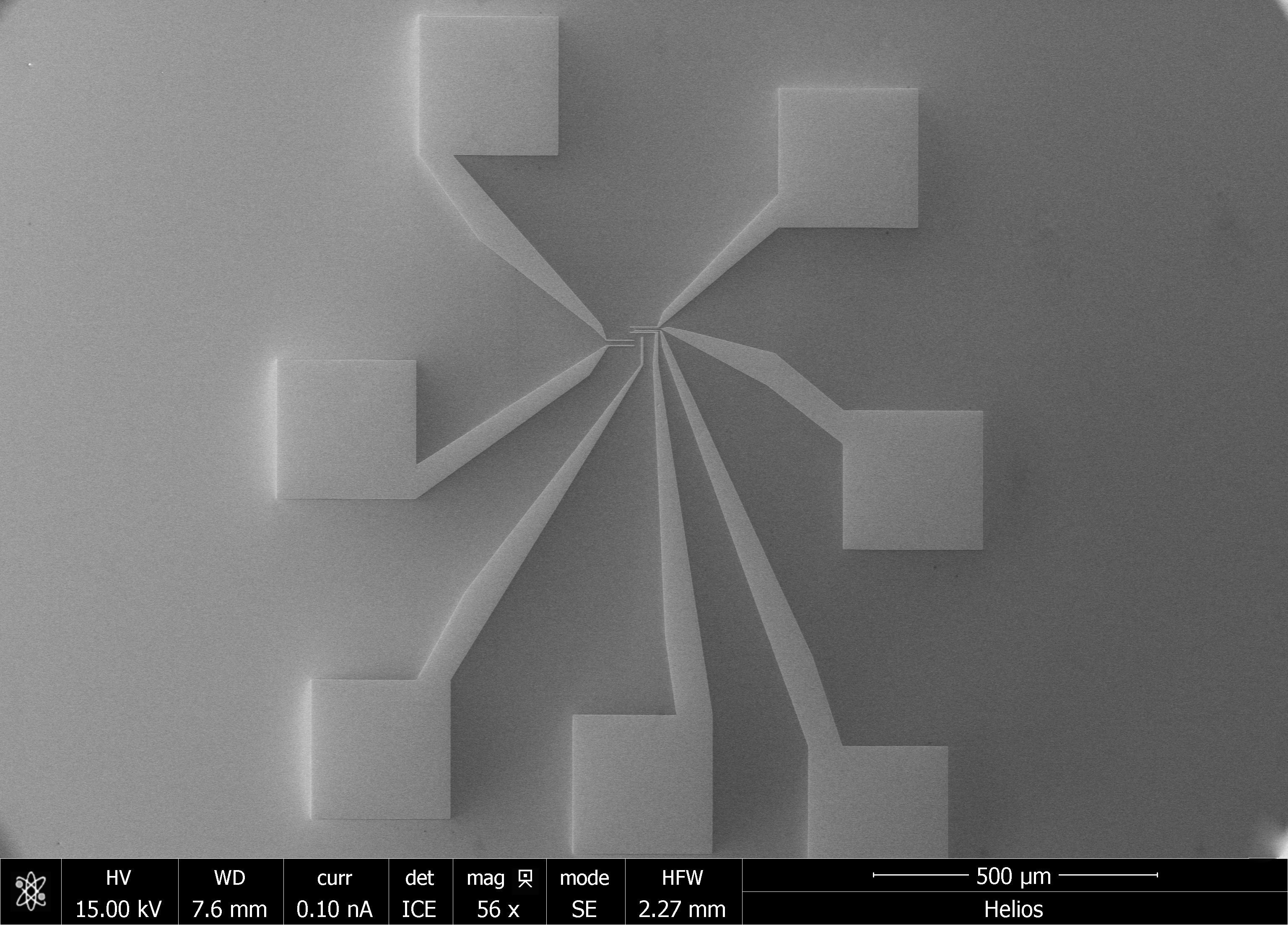 Material Science
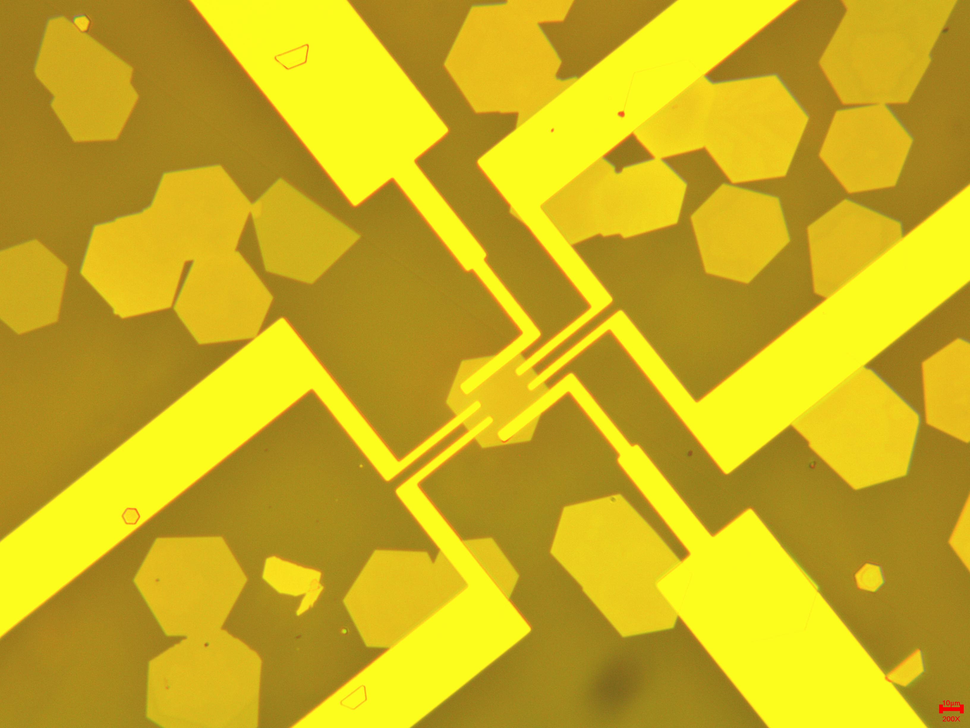 Material Science
 Material Science
 Material Science
 Micro
Micro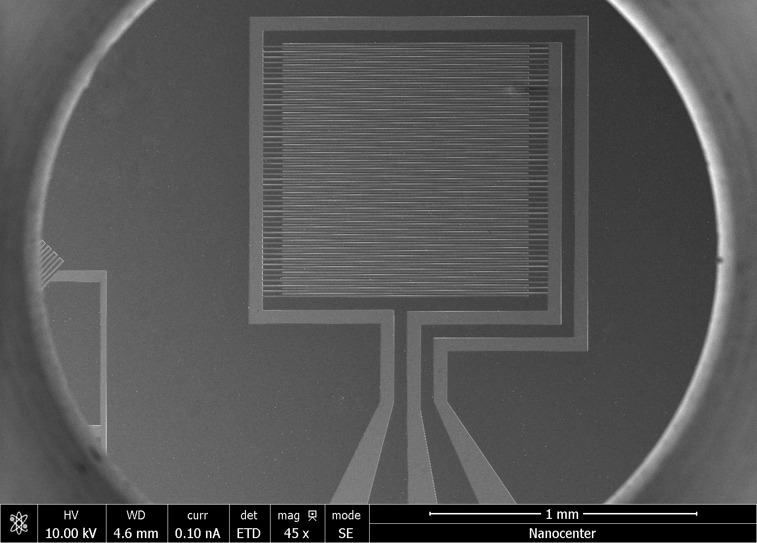 Micro
Micro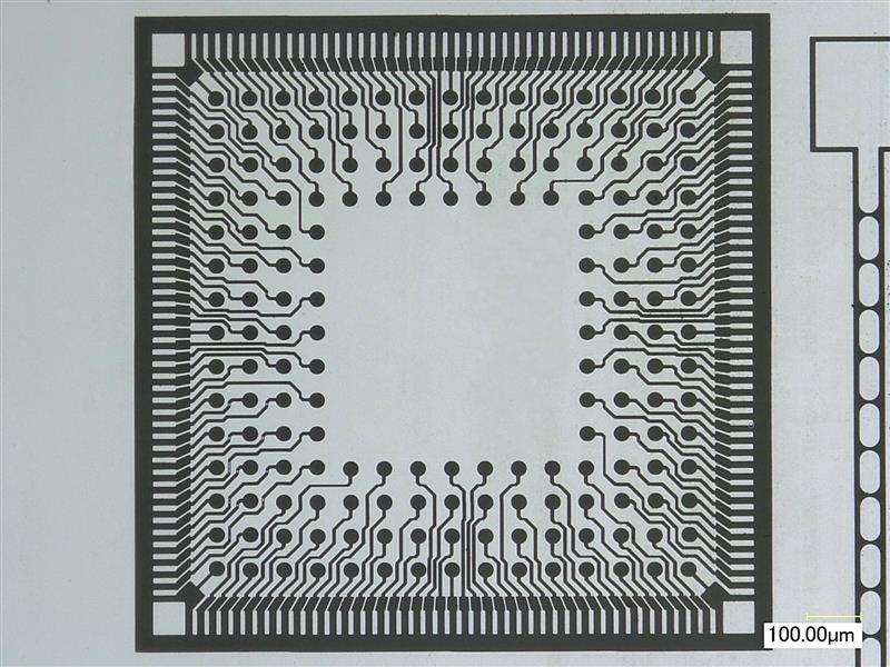 Micro
Micro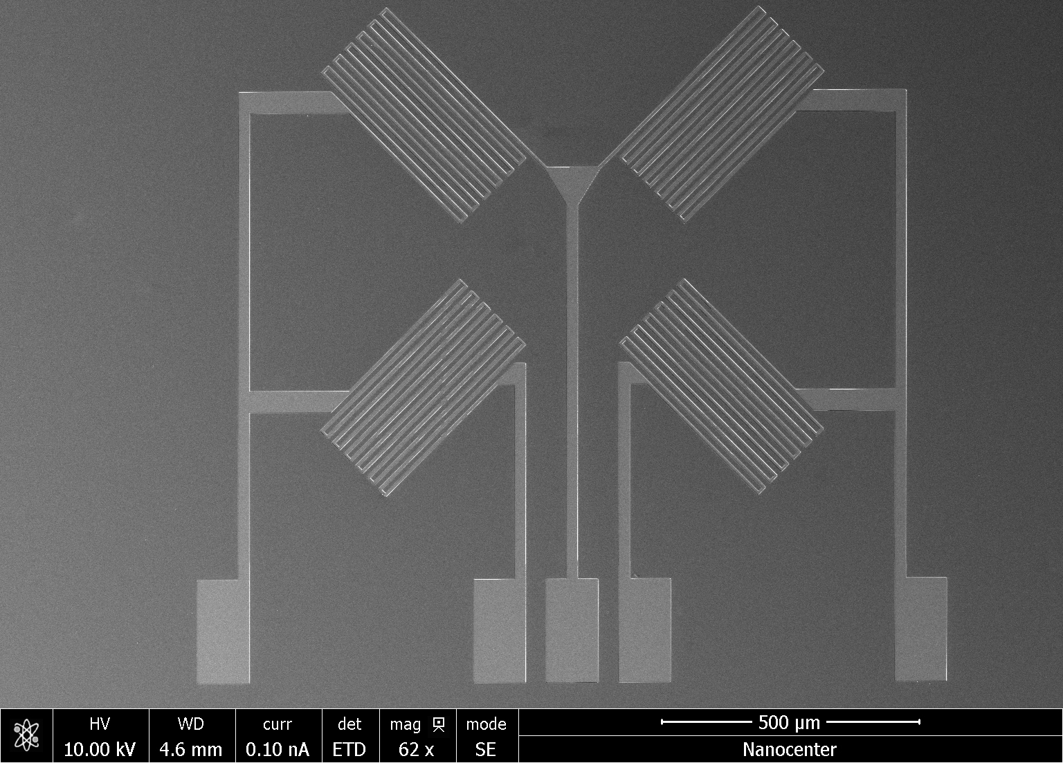 Micro
Micro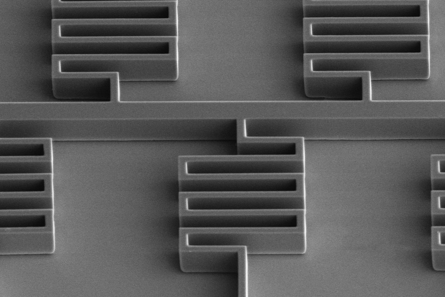 Microfluidics
 Microfluidics
 Microfluidics
 Microfluidics
 Microfluidics
 Microfluidics
 Microfluidics
 Microfluidics
 Microfluidics
 Microfluidics
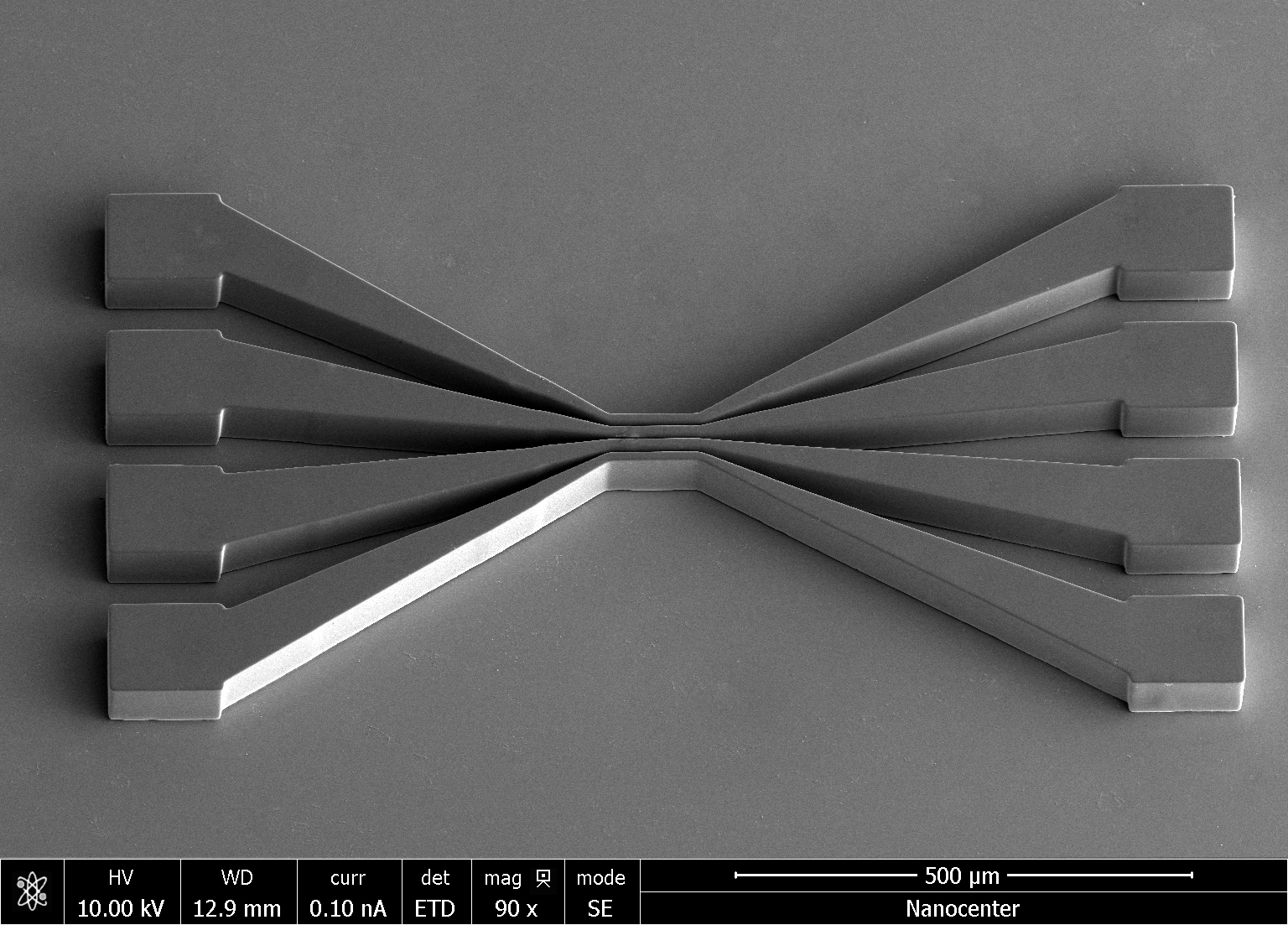 Microfluidics
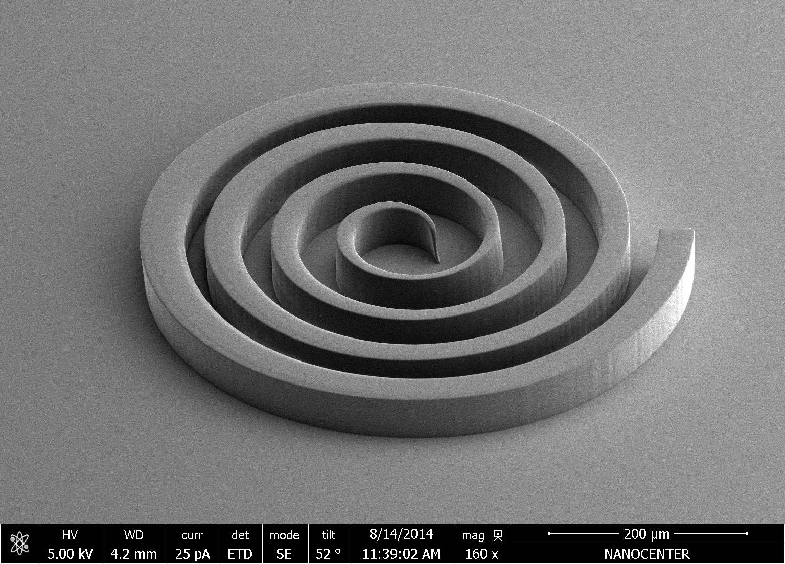 MEMS
MEMS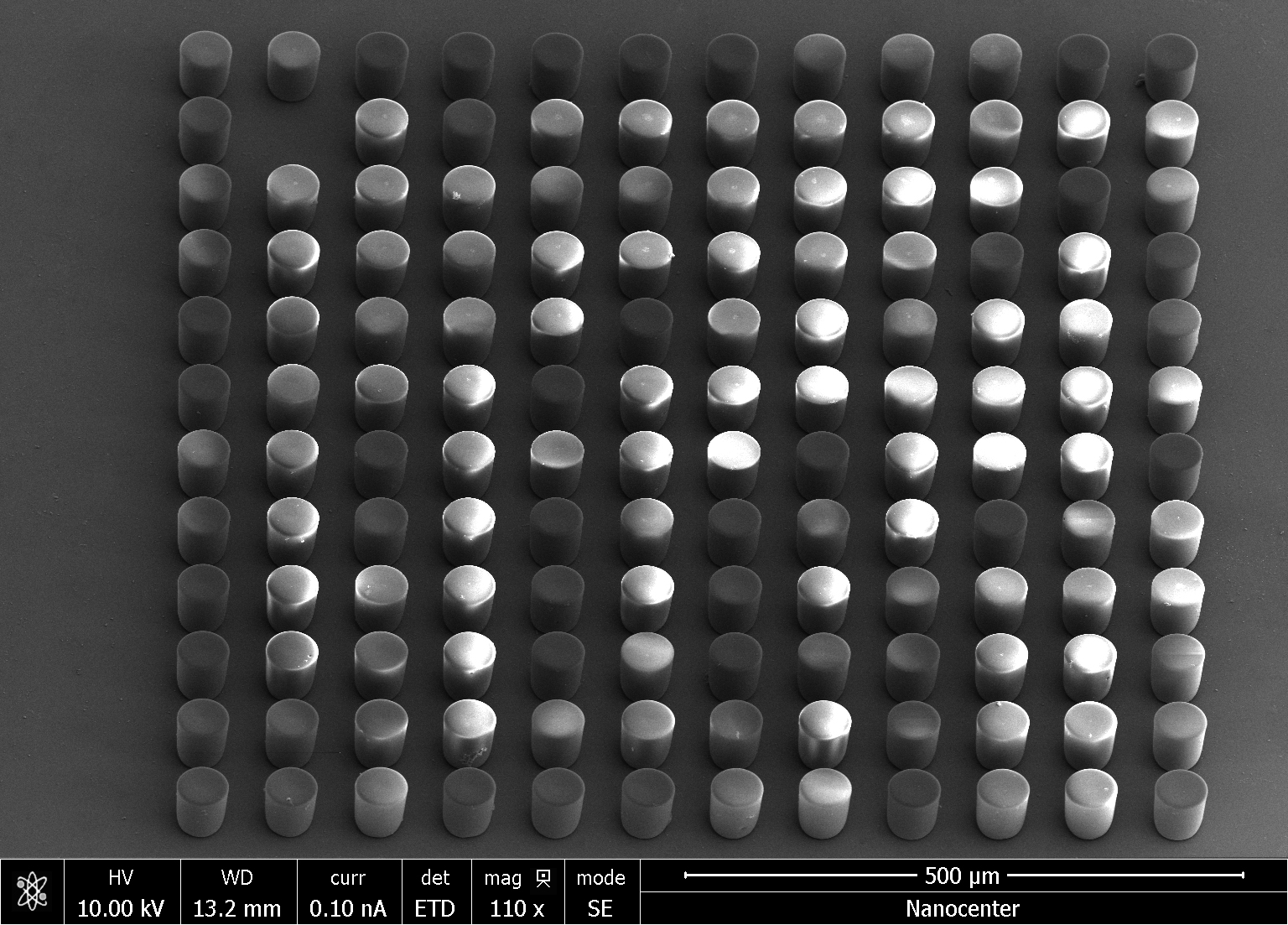 MEMS
MEMS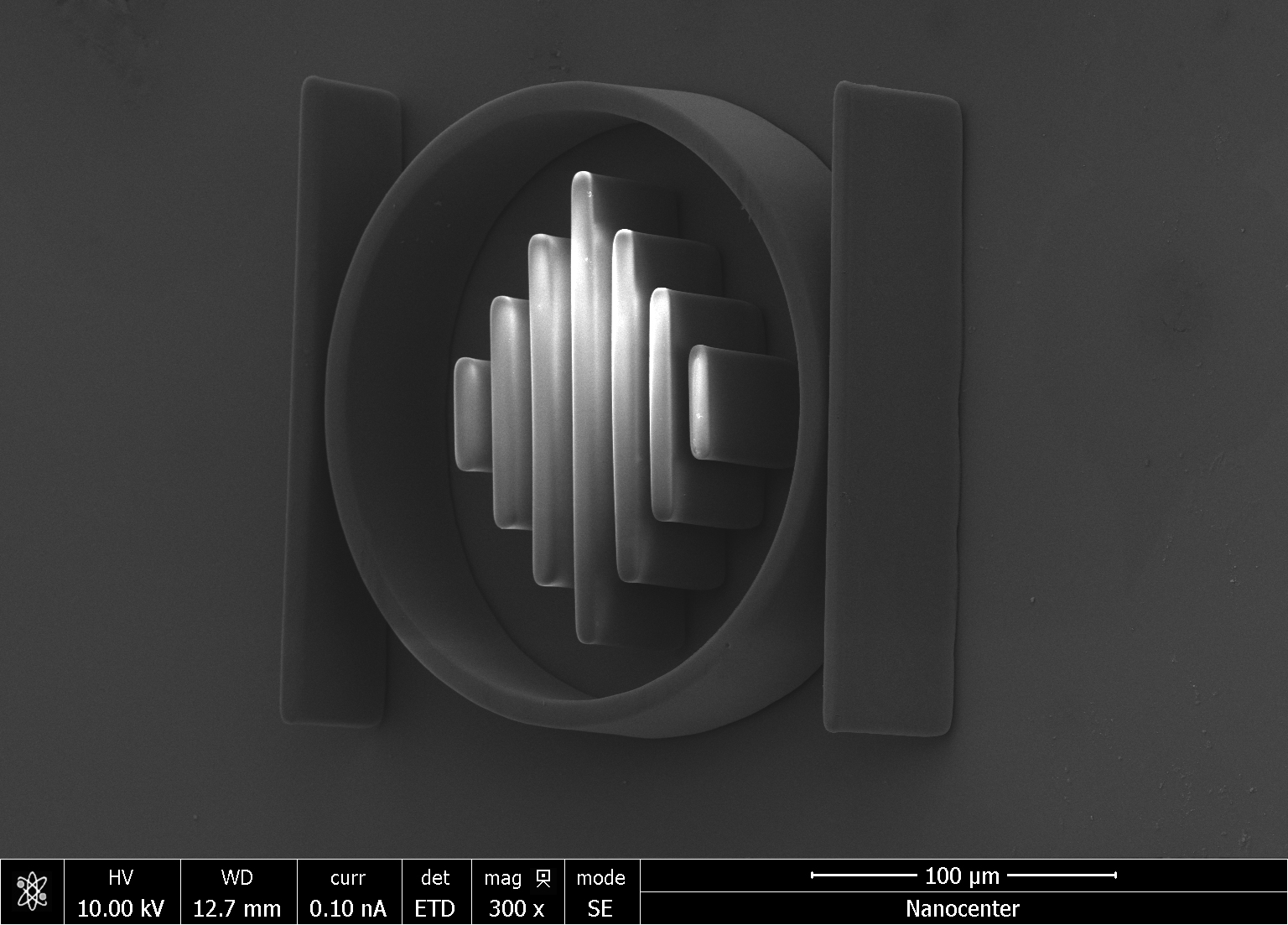 MEMS
MEMS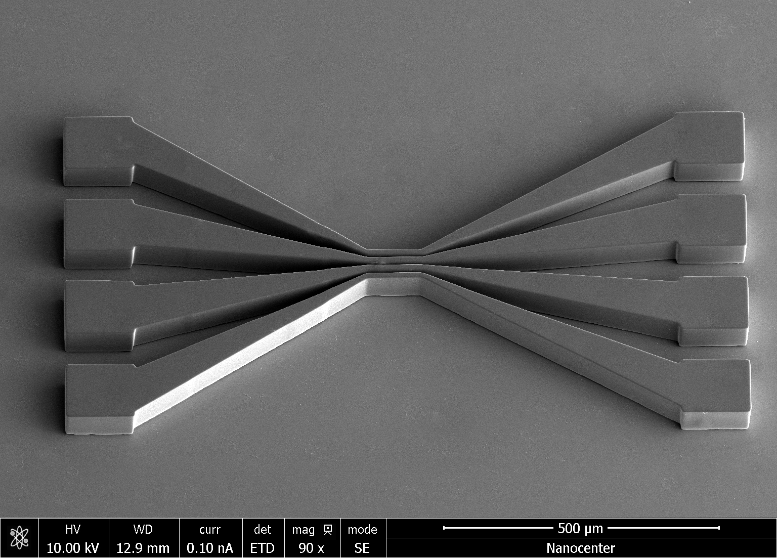 MEMS
MEMS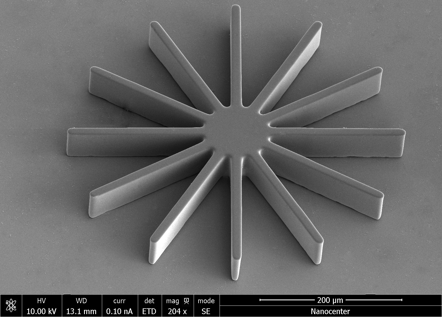 MEMS
MEMS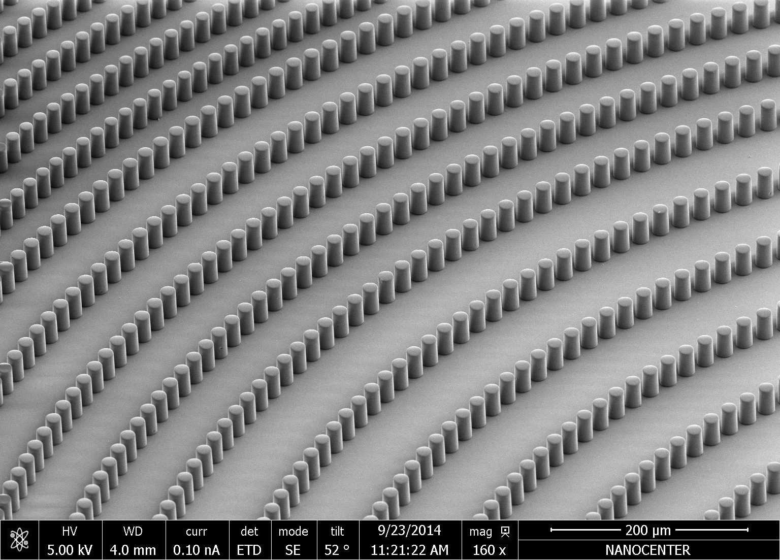 MEMS
MEMS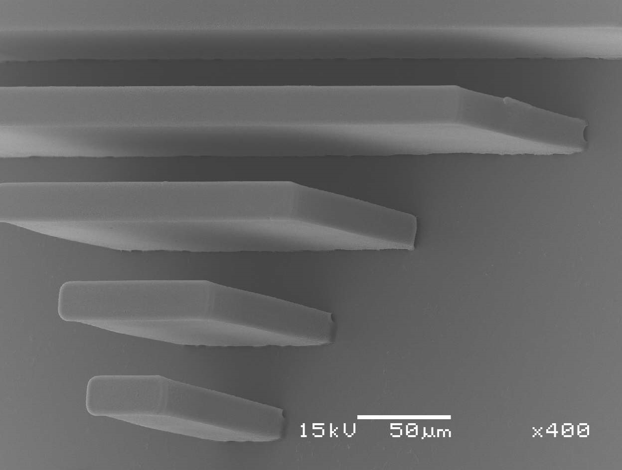 MEMS
MEMS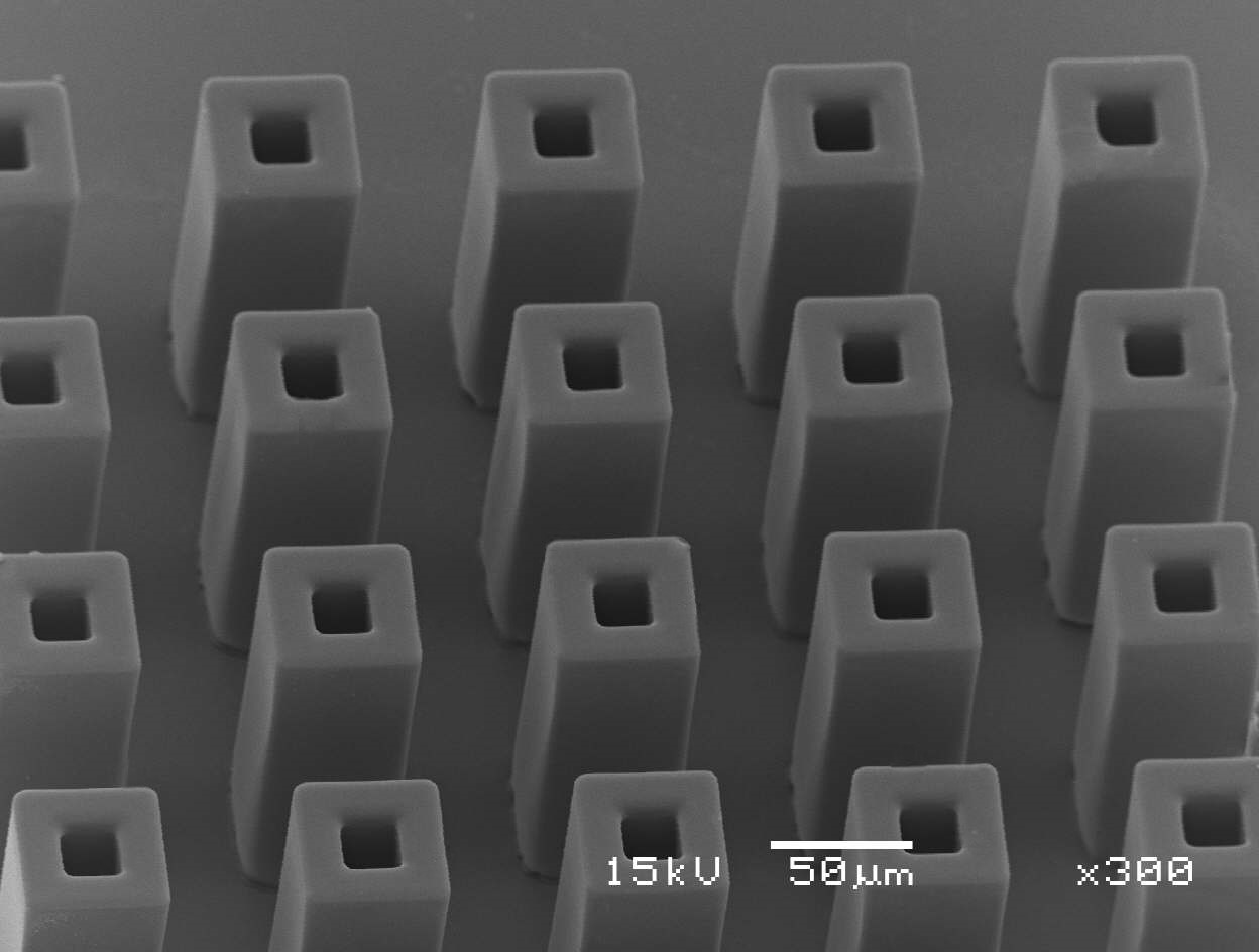 MEMS
MEMS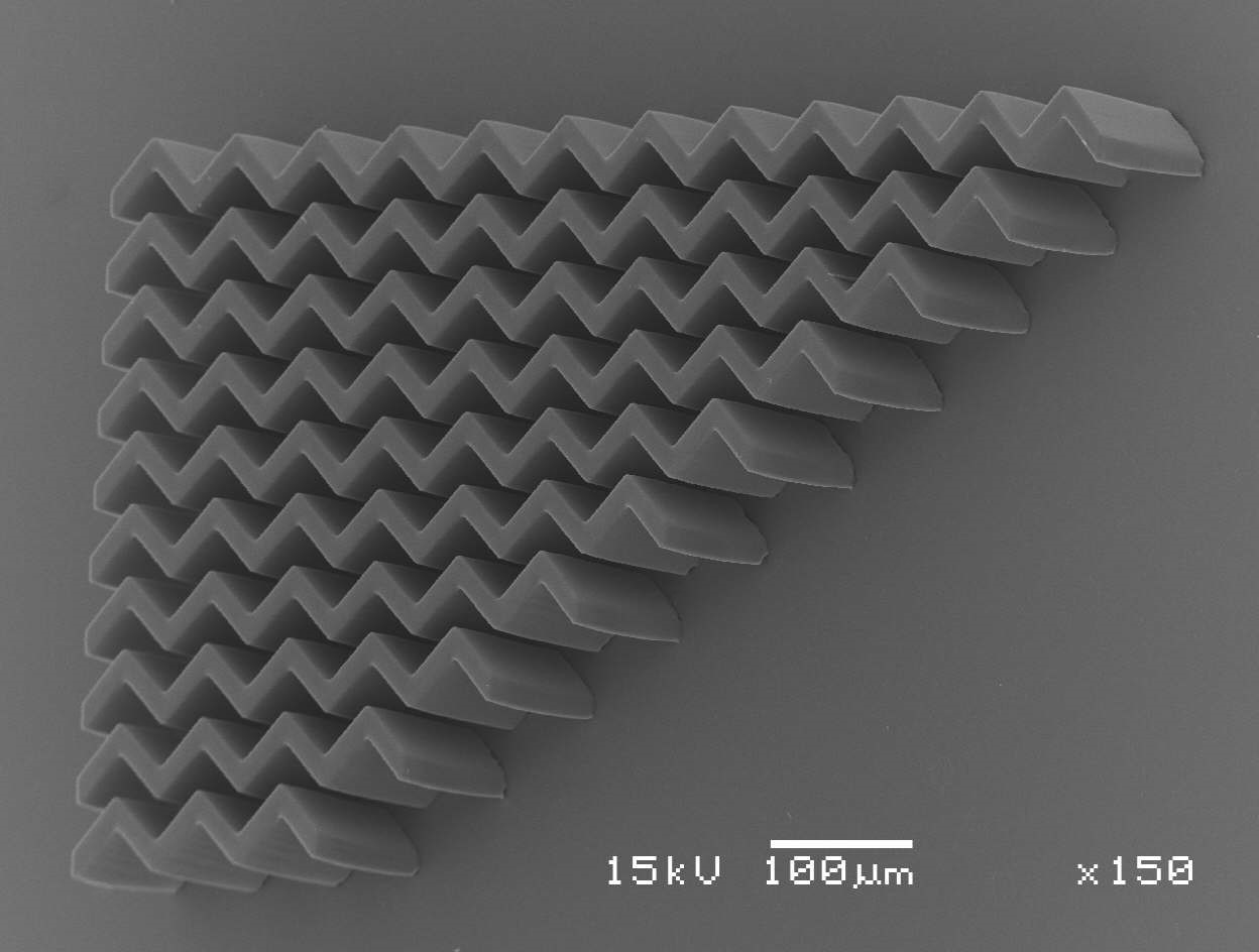 MEMS
MEMS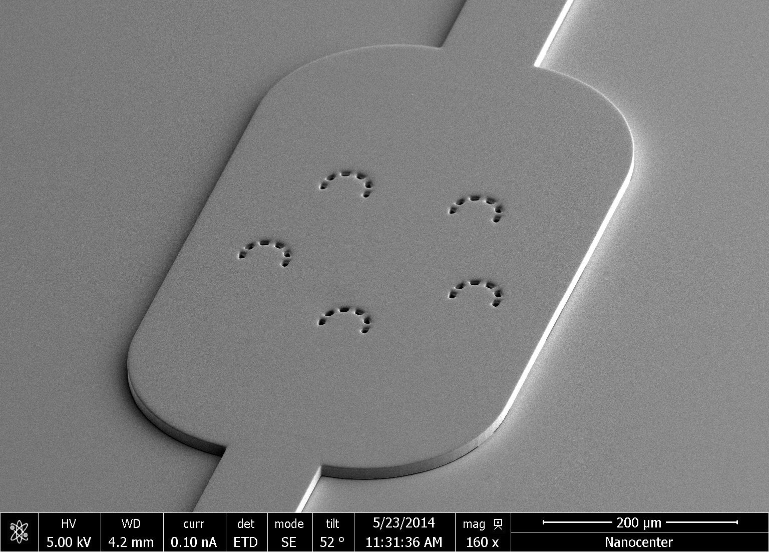 MEMS
MEMS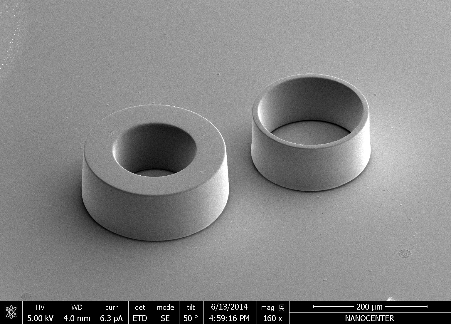 MEMS
MEMS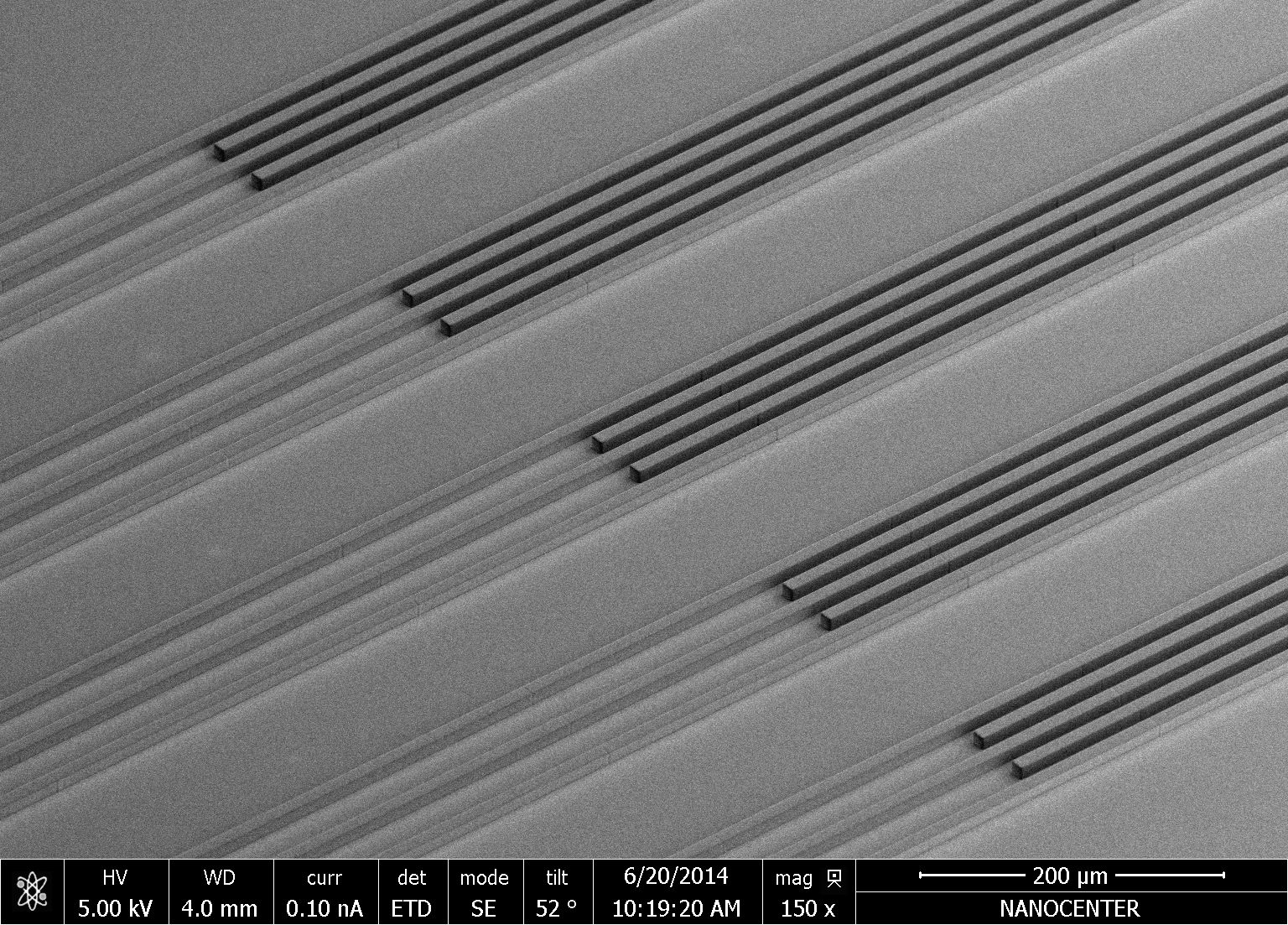 MEMS
MEMS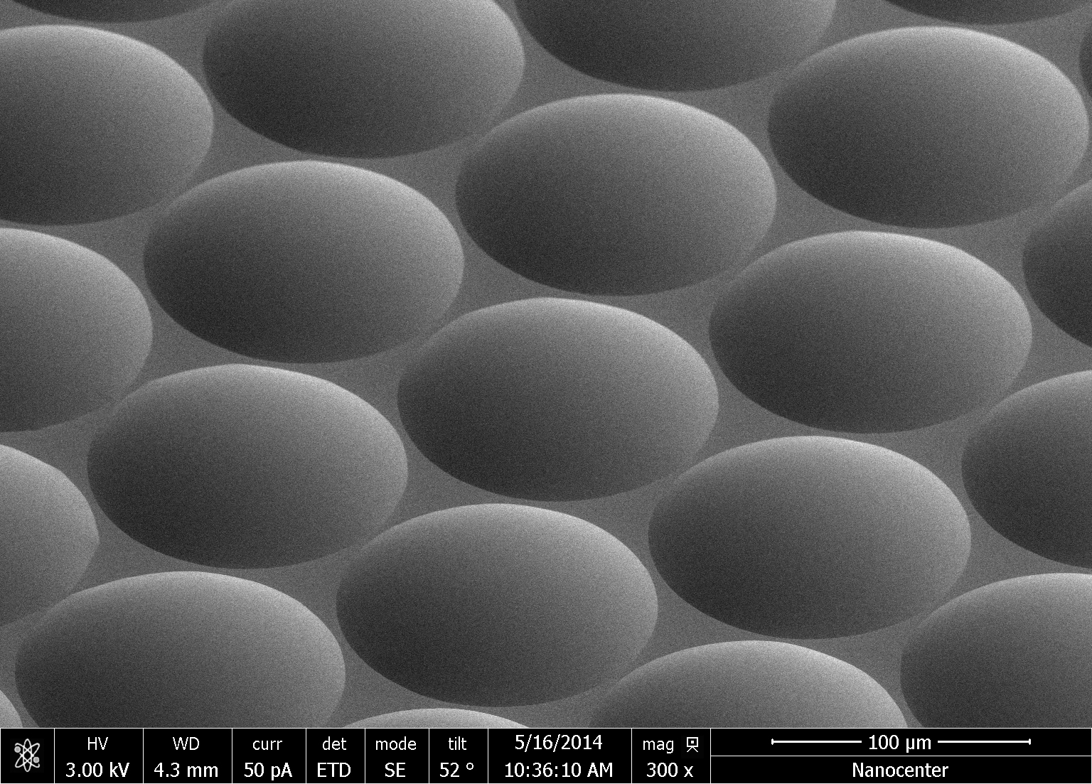 MEMS
MEMS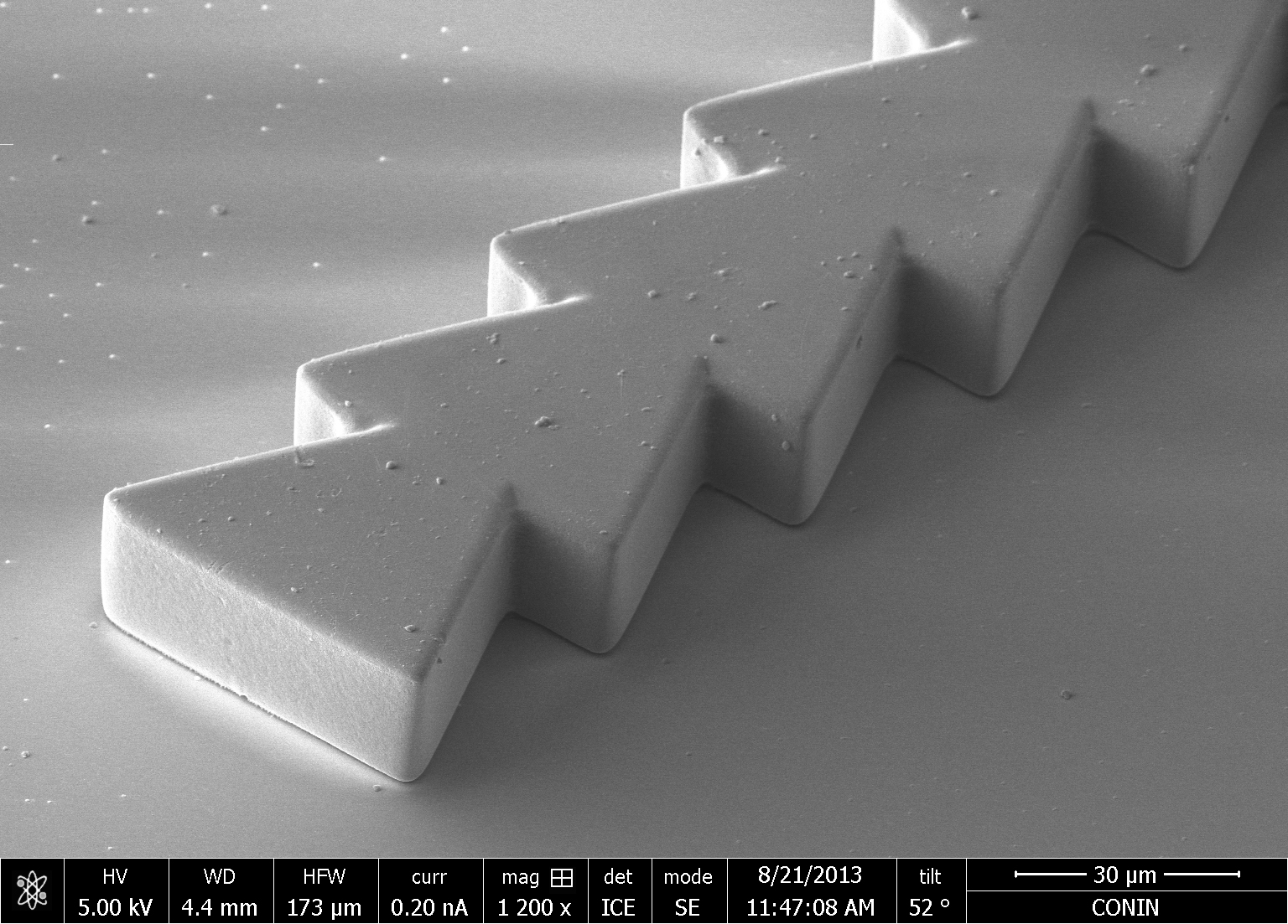 MEMS
MEMS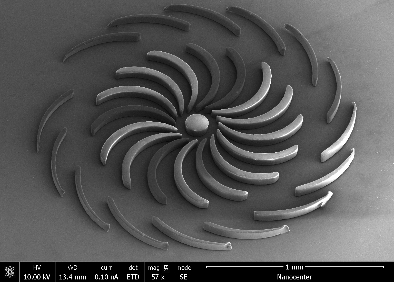 MEMS
MEMS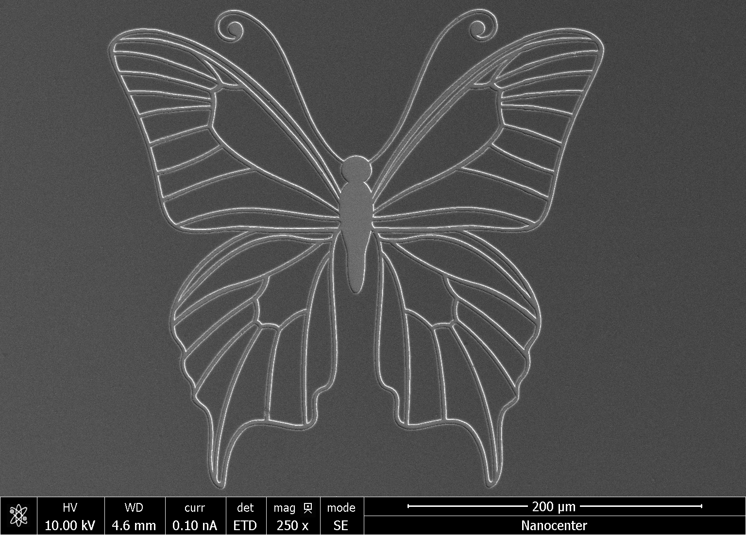 Bio Physics
Product Information Notice
Product information on this website represents potential capabilities of suitably configured scientific research systems. Exact specifications, supported techniques, performance, availability and configuration depend on the manufacturer, model and installed accessories. Contact Adepth Consulting Engineers for configuration-specific information.