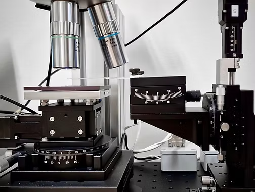


2D Material Detection and Transfer System
Automated tool that uses computer vision, machine learning, and optical microscopy to find, classify, and map atomically thin flakes like graphene. With precision mechanical and optical tool used to pick up and stack two-dimensional atomic crystals like graphene.

2D Material Detection and Transfer System
A 2D (two-dimensional) semiconductor material is a crystalline solid that is only one or a few atoms thick, that controls electrical current like traditional semiconductors. These materials extend wide in length and width, but they have almost zero thickness in the third dimension. Because they are so thin, electrons can only move in a flat plane. This restriction changes how the material behaves compared to normal, thick materials. 2D material detection and transfer system uses automated optical microscopy and micro-positioning stages to locate, align, and deterministically place atomically thin flakes like graphene onto target substrates.
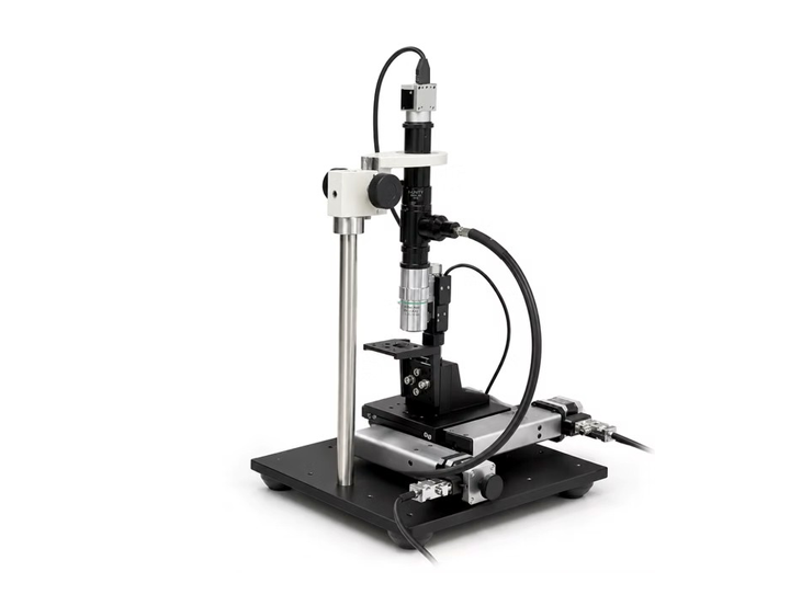
2D Material Detection System
Sejong 2D Material Detection System, is an automated tool that uses computer vision, machine learning, and optical microscopy to find, classify, and map atomically thin flakes like graphene and transition metal dichalcogenides (TMDCs). They measure less than a micrometer thick vertically, existing as flat, sheet-like layers.
Automated Scanning, eliminates the time-consuming manual search and documentation under optical microscopes. AI & Deep learning uses Convolutional Neural Networks (CNNs) to distinguish target materials from surface contaminants. Compatible with all 2D materials, even unknown van der Waals crystals. Thickness & Shape Mapping, instantly calculates optical contrast to estimate layer counts (such as monolayer vs. multilayer), dimensions, and spatial coordinates. Database Integration, Stores high resolution flake images and coordinates in interactive libraries to streamline device fabrication.
Key advantages of Sejong 2D Material Detection System
- Max Scan range: 5cm x 5cm
- Objective lens: 10x, 20x, 50x, all compatible
- Materials: Graphene, hBN, TMDC, MXene, etc., including all 2d materials
- Substrate: SiO2/Si, glass,
- Detection speed: 1.3 sec/frame
- Scan speed: 0.5 um^2/sec.
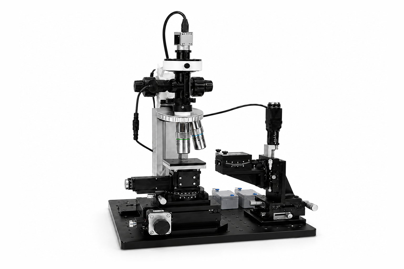
2D Material Transfer System
Sejong 2D Material Transfer System is a precision mechanical and optical tool used to pick up and stack two-dimensional atomic crystals like graphene. An essential tool in fabricating devices using van der Waals (vdW) materials in a 2D material transfer setup. This system allows precise placement of selected 2D material flakes onto desired locations on a substrate. Building such a setup is critical for encapsulating air-sensitive materials like graphene and other vdW materials within stable dielectrics such as hexagonal boron nitride (hBN) and mica, ensuring their stability for characterization and use in ambient conditions.
In some applications, the 2D material transfer process is also used to fabricate devices by placing vdW flakes onto pre-patterned electrodes, eliminating the need for exposing these sensitive materials to chemicals, high temperatures, and other processes involved in traditional lithography and nanofabrication techniques. This approach preserves the pristine properties of the vdW materials, which is especially important for materials like magnetic vdW heterostructures.
Automatic detection and localization of 2D materials prior to transfer, with Z-axis motorized, (optional motorized XY axis), Stamp stage offers, accurate speed, distance control through software. Heater Stage of 80 mm × 80 mm allows heating up to 200 °C with PID Temperature Control through software. Vacuum chucks, secure wafer handling during the pickup and transfer process. With a spacious stage capable of holding up to five vacuum chucks, multiple 2D materials can be prepared simultaneously. This unique design significantly streamlines the fabrication of van der Waals heterostructures, enabling researchers to quickly alternate between different materials and build complex multilayer devices with maximum efficiency.
Rotation stage for sample (optionally motorized): compatible for "Tear-and-Stack" method alternate between different materials and build complex multilayer devices with maximum efficiency and for twisted van der Waals heterostructures (0.1° rotation accuracy guaranteed ) With Tilt stages (Goniometer and Rotation stage of 4 & 7 axis options) for stamp and compact design allowing installation in a glove box for air sensitive materials.
Key advantages of Sejong 2D Material Transfer System
- Max Sample scan range: 5cm x 5cm
- Objective lens: 20x(basic), 10x, 50x
- Substrate: SiO2/Si, glass
- Detection Speed: 1.3 sec/frame
- Stamp Stage Z-Scan speed: 1 - 1000 µm/sec.- Sample Stage Speed: 2500 µm/sec.